Performance of fibre laser process for industrial application
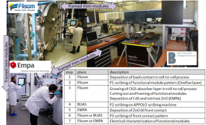
Partners: BUAS (Switzerland), ONEFIVE (Switzerland), EMPA (Switzerland), FLISOM (Switzerland)
For the present assessment case of laser scribing of thin-film solar cells on a flexible substrate, this involves that the optical scribing unit should work reliably without the need for human intervention during the experimental period. Scribing process parameters determined during preliminary experiments were not re-adjusted at least within one production batch. Production of thin-film samples should be done on a production line or at least a pilot line. Scribing must be done at industrially relevant throughput. Performance of the scribing processes developed in APPOLO was directly compared to industrial reference samples produced using existing production processes. Sample characterisation has been done according to quality measurement standards of the end-user.
Workflow used in APPOLO assessment experiments
 Results:
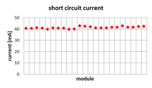
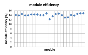
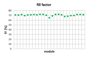
- The efficiency of 15 percent was reached on industrial samples using standard APPOLO patterning without lowering the scribe-separation.
- A comprehensive series of assessment experiments have been conducted on Flisom’s pilot line and partially on APPOLO scribing machine.
- Suitability of APPOLO processes for the industrial production of CIGS thin-film solar cells has been demonstrated.
Scribing performance of the system with polygon scanner
Partners: FTMC (Lithuania), LUT (Finland), EKSPLA (Lithuania), NST (Belgium), AMSYS (Israel), ELAS (Lithuania), FLISOM (Switzerland), EMPA (Switzerland)
The investigated CIGS scribing regimes.
In the frames of the APPOLO project, different scribing approaches were investigated for CIGS module structuring. The P3 “type 1” regime involved direct laser ablation of the TCO and absorber material to expose the molybdenum back-contact. In this case, high pulse overlap regime is required. Therefore, there is a large chance of heat accumulation during the scribing. However, these issues are less critical in the case of P2 scribing (interconnect formation). For this, the P3 process parameters can be easily adapted for the P2 scribing. The P3 “type 2” involved removal of the front-contact only. That is a low pulse overlap regime, and laser-induced thermal effects can be reduced.
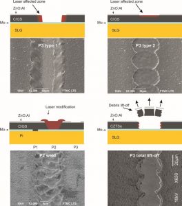
Laser scribing process types investigated in the APPOLO project
Laser-scribing of P2 for Perovskite PV for optimal interconnection fabrication
Partners: IOM (Germany), UPM (Spain), EMPA (Switzerland), FLISOM (Switzerland)
The activities of WP3 were restructured due to the extension of the work to laser scribing of perovskite films as a new exciting absorber material for thin film photovoltaics. The workplan was reorganized, and a new end-user (FLISOM) was incorporated. The main work done is based on one future vision related to the activities of the end-user, which is currently focused on the fabrication of flexible thin film CIGS solar modules, to combine CIGS and perovskite solar technology for R2R tandem module fabrication. This approach can significantly increase the efficiency of solar modules, which is the fundamental parameter in being competitive with silicon PV at least for applications that require flexible solar modules. One crucial part of the work concentrated on the optimization of the thin film stack for perovskite solar cells including the development of the suited fabrication technologies of the particular films for a semi-transparent solar cell design. Therefore, the usually used gold back contact was replaced by a TCO layer to achieve the transparency of the solar cell up to the band gap of the absorber. In particular, the deposition techniques were adapted to avoid damage to the absorber within the TCO deposition process. Furthermore, additional materials suitable for a transparent conductive layer were chosen and optimized. The laser-based scribing process of the perovskite film was studied in more detail to gain the understanding of the laser-photon perovskite-film interaction process in relation to the best characteristics of the laser scribing for the integrated interconnection process of modules fabrication. Two ablation mechanisms have been observed in general: the standard laser ablation due to fast evaporation/decomposition of the material and a lift-off process due to laser-driven interface phenomena. Both processes were observed for the studied laser irradiation directions – film and substrate side irradiation – and for the examined laser sources. Low laser threshold fluences for patterning were found for photon energies above the band gap or ultrashort laser pulses. For those laser processing conditions, a selective scribing can be achieved without damaging the substrate including deposited films (TCO).
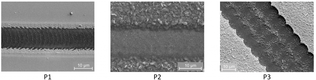
SEM images of the three scribes required for integrated interconnection P1, P2, and P3 with ps laser UV pulses
Laser-based metallization of full-size solar cells by LIFT
Partners: UPM, MONDRAGON ASSEMBLY, ABENGOA
The laser-induced forward transfer (LIFT) process is a technique to transfer locally different materials and in different sizes onto a number of different substrates. The laser beam is focused in the donor substrate/ribbon interface. During the pulse duration, the laser energy is deposited within the laser spot size into the interface, evaporating a little amount of the material and generating the expansion of the remaining material, accelerating the non-evaporated part of the metal film towards the acceptor substrate.
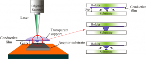
Principle of LIFT process for metallisation of thin-film solar cells


